
ESD Packaging Solutions for Semiconductor & Electronics Manufacturing
Malaster provides ESD-safe packaging solutions for sensitive semiconductor devices, electronic components, wafers, and assemblies. Our standard and custom packaging systems are designed to support reliable handling, storage, manufacturing, and transport while helping protect components from electrostatic discharge, physical damage, and contamination.
Solutions include JEDEC trays, IC shipping tubes, wafer packaging, conductive and static-control materials, and
custom thermoformed ESD trays
engineered around specific component and handling requirements.
Packaging Built Around the Application
For more than 30 years, Malaster has supported semiconductor, electronics, aerospace, medical technology, telecommunications, and other high-reliability industries with packaging solutions ranging from readily available standard products to fully engineered custom systems.
Core Capabilities
ESD Material Options:
Conductive, static dissipative, and antistatic materials are available for a wide range of component handling and protection requirements.
Custom Engineering:
Packaging can be developed around component geometry, cavity layout, material thickness, handling method, storage requirements, and shipping conditions.
Semiconductor Packaging:
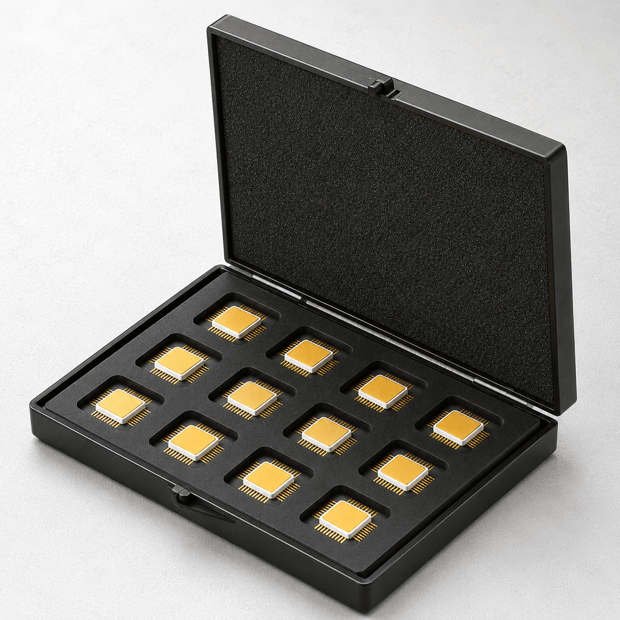
Solutions include JEDEC trays, IC shipping tubes,
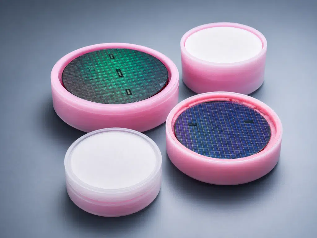
wafer shippers,
conductive foam, thermoformed trays, and related ESD packaging systems.
Compliance-Conscious Materials:
Material options are available to support RoHS and REACH requirements where applicable.
Whether the requirement calls for an established packaging format or a custom solution designed around a specific device, Malaster helps customers select packaging that fits the product, process, and application.
Industries & Applications
Malaster supports industries where sensitive electronic components must remain protected throughout manufacturing, handling, storage, and shipment. Our ESD packaging solutions are used across semiconductor production, aerospace and defense, medical technology, telecommunications, and other electronics applications where component integrity is critical.
Semiconductor & Electronics Manufacturing
Semiconductor devices, integrated circuits, wafers, and electronic assemblies require controlled handling throughout production and distribution. Malaster provides packaging designed to protect these components while supporting practical manufacturing and material-handling workflows.
-
Integrated Circuits & Components:
ESD packaging for integrated circuits,
transistors, microchips, and other sensitive devices.
-
Wafer Handling:
Wafer shippers, wafer jars, separators, foam, and related packaging for semiconductor wafers.
-
Production Packaging:
JEDEC trays, IC tubes, thermoformed trays, conductive materials, and custom component packaging.
Aerospace & Defense
High-reliability aerospace and defense electronics require dependable packaging during storage, assembly, transport, and supply-chain handling.
-
Packaging for avionics components, sensors, control electronics, modules, and related assemblies.
-
Custom material and packaging configurations for specialized component geometries and handling requirements.
-
ESD-safe solutions for controlled and compliance-conscious manufacturing environments.
Medical Devices & Diagnostic Equipment
Medical electronics, sensors, diagnostic systems, and electronic assemblies often require both ESD protection and careful physical handling.
-
Protective packaging for sensitive medical and diagnostic electronics.
-
Material options suitable for controlled manufacturing and handling environments.
-
Custom configurations developed around device dimensions, storage, handling, and transport requirements.
Telecommunications & Network Electronics
Malaster packaging solutions support the handling and movement of sensitive communications and network components throughout manufacturing, deployment, and distribution.
-
Packaging for communication modules, electronic assemblies, network hardware, and related components.
-
Custom-fit solutions for unusual dimensions or specialized handling requirements.
-
Packaging suitable for domestic and international distribution environments.
Other ESD-Sensitive Applications
Our standard and custom packaging solutions can also support industrial electronics, instrumentation, sensors, research applications, and other products where electrostatic discharge or physical handling damage presents a risk.
Why Choose Malaster for ESD Packaging?
Effective ESD packaging is not simply about putting a component into a conductive container. The material, geometry, fit, handling method, and shipping environment all influence how well a packaging system performs.
Malaster combines established ESD packaging products with custom engineering capabilities, allowing customers to select an existing solution when one fits or develop a purpose-built package when it does not.
Reliable ESD Protection
Our
ESD packaging solutions
are available in conductive, static dissipative, and antistatic materials selected for the requirements of sensitive semiconductor and electronic components.
-
Controlled Materials: Material options for a range of ESD-sensitive handling applications.
-
Physical Protection: Packaging designed to help stabilize, separate, and protect components during handling and transport.
-
Broad Component Support: Solutions for integrated circuits, wafers, PCBs, electronic assemblies, and other sensitive devices.
Custom Engineering When Standard Packaging Is Not Enough
Some components simply do not fit an existing tray, tube, box, or carrier. Malaster can develop packaging around the actual device and the way it will be handled.
-
Custom Dimensions: Sizes, cavity layouts, material thicknesses, and configurations developed for the application.
-
Application-Specific Design: Packaging designed around manufacturing, storage, automated handling, or shipping requirements.
-
Identification Options: Custom labels, markings, printing, and other identification features are available for selected packaging systems.
Standard Products and Custom Solutions from One Source
Malaster supplies a broad range of semiconductor and electronics packaging, including JEDEC trays, IC shipping tubes, wafer packaging, conductive foam, thermoformed trays, ESD bags, protective boxes, and related accessories.
This combination of stocked products and custom capability makes it easier to match the packaging approach to the requirement instead of forcing the requirement into a single product category.
Experienced Technical Support
With more than 30 years serving the electronics industry, Malaster can help evaluate packaging requirements, identify existing options, and determine when a custom solution is the better approach.
Find the Right ESD Packaging Solution
Whether you need a standard packaging product or a custom solution engineered around a specific component, Malaster can help identify the right approach for your application.
Start with Your Packaging Requirement
Tell us what you are packaging, how the component will be handled, and any material, dimensional, storage, or shipping requirements that need to be considered.
-
Looking for an existing product? Browse our semiconductor and electronics packaging solutions by product category.
-
Need help selecting a package? Our team can help identify compatible trays, tubes, wafer packaging, foam, and other ESD-safe products.
-
Need something custom? We can evaluate custom thermoformed trays and other engineered packaging configurations for specialized applications.
You can also explore our
technical resources
for guidance on ESD packaging, component handling, materials, and product selection.